Polishing Pad Business
Extremely precise polishing processes are essential for advanced products such as semiconductor devices,
and Fujibo Ehime's ultra-high precision polishing pads make this possible.

Feature


Ultra-high precision polishing pads which support the coming of an IoT (Internet of Things) society
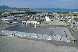
Our polishing pads have high market share in many precision polishing pad fields, including: LCD glass essential for smartphones, tablets and LCD TVs, hard disks for storage devices, and silicon wafers for semiconductor substrates and semiconductor devices. The Polishing pads business started in Nyugawa, Ehime Prefecture, and has now expanded into five plants, adding: Oita in Oita Prefecture, with Oyama in Shizuoka Prefecture, Kozakai in Aichi Prefecture and Tainan in Taiwan. As a core business of the Fujibo Group, it will continue to develop its overwhelming production capacity and the organization system where sales, development, manufacturing and quality assurance departments work together to provide products and services.

Our
Advantage
-
Customization
We provide polishing pads that meet customer demand by sales, development, manufacturing and quality assurance departments working together to understand customer needs and develop products.
-
R&D
CapabilityOur R&D capability with our analysis and polishing evaluating technologies developed through many years of experience enables us to provide products that meet customer demand.
-
Production
CapacityWe have the highest manufacturing capacity of polishing pads in the industry with 5 plants (4 in Japan and 1 in Taiwan) which enables us to completely follow the BCP.
"User in customization"
to always meet user requests
Our Advantage - 01. Customization
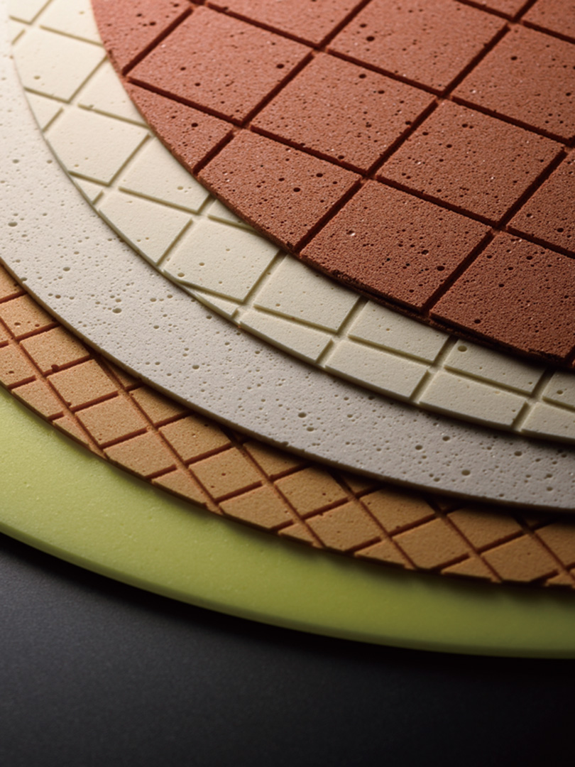
Achievement as a specialist in development of polishing pads

The Fujibo Group has R&D achievements in almost all applications of polishing pads and satisfies customer needs with accumulated expertise and flexible customization.

Provision of solutions as a team

Our sales, development, manufacturing and quality assurance departments all work together to solve customers' issues and problems and to provide the best products and services to meet their needs.
R&D system to sufficiently meet customer needs
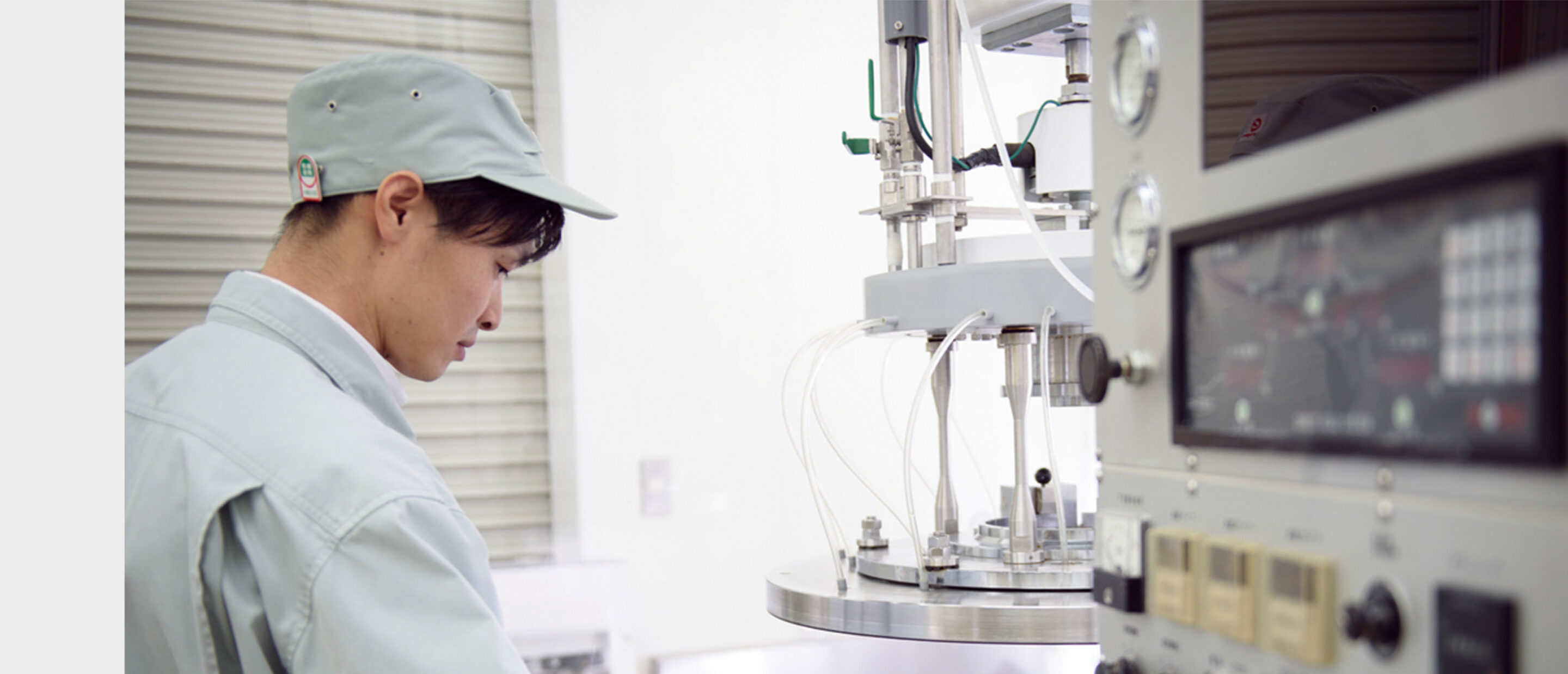
Our Advantage - 02. R&D Capability
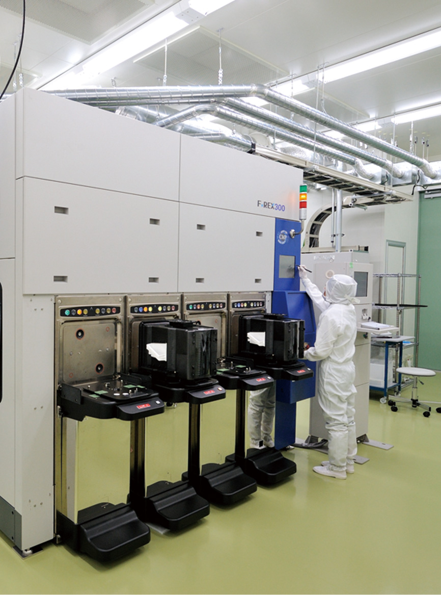
R&D system with cutting-edge polishing evaluation facilities

We have introduced state-of-the-art polishing evaluation facilities to achieve polishing performance that customers demand. It enables us to propose solutions by replicating and verifying the polishing evaluation processes implemented by our customers.
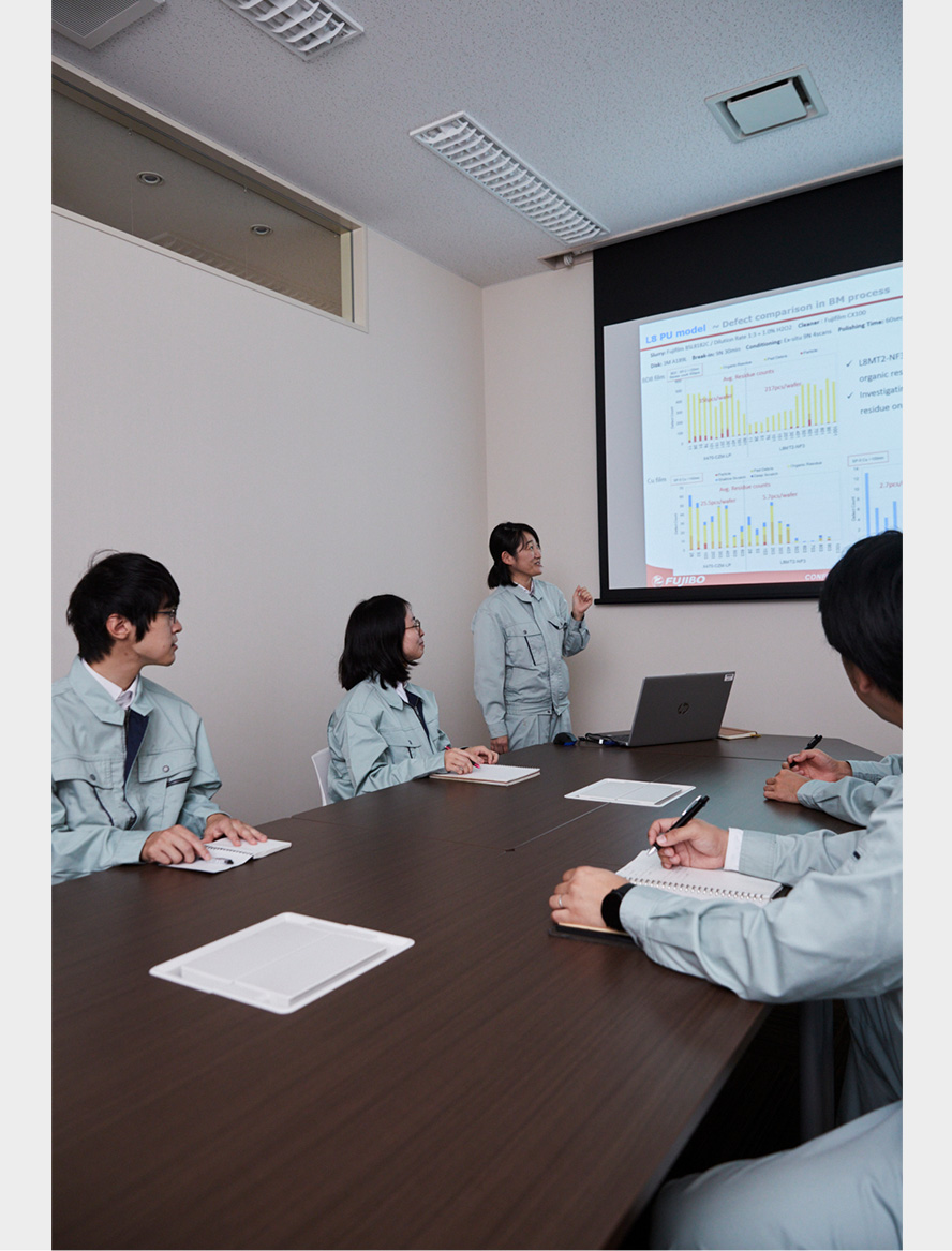
R&D from customer's viewpoint

Our sales, development, manufacturing and quality assurance departments work together to understand customer needs more accurately and develop products and to provide customers with services.
5 plants in and outside Japan with the highest scale in the industry
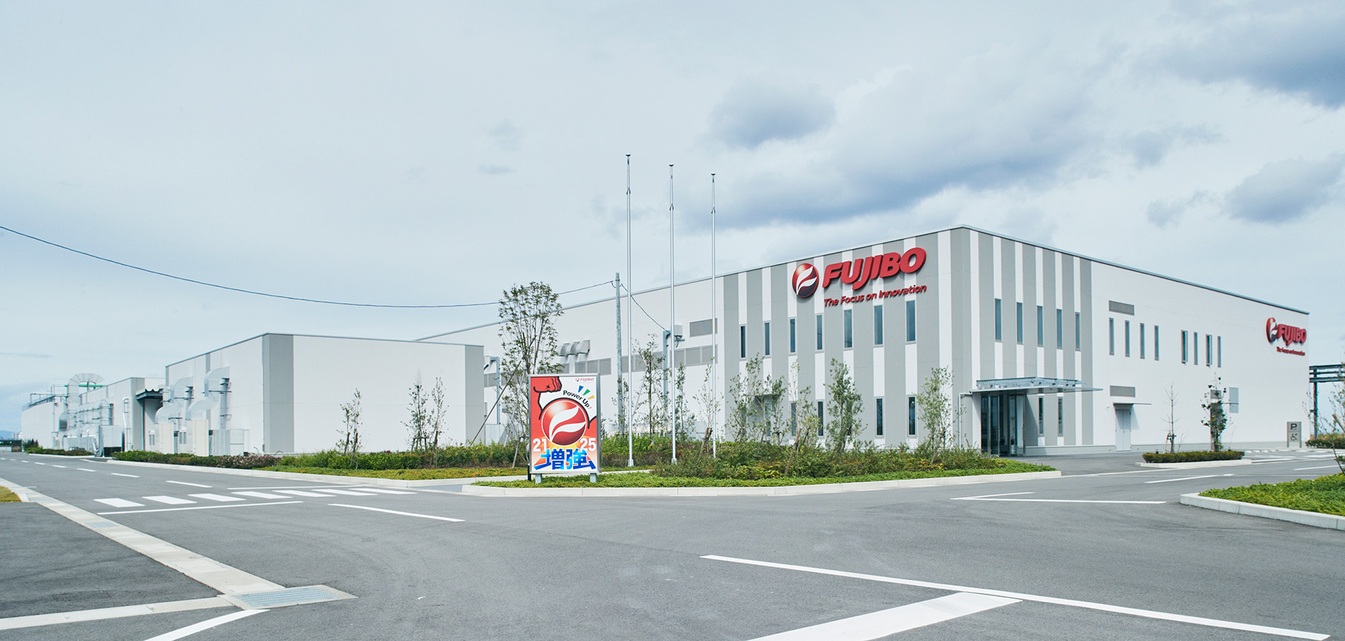
Our Advantage - 03. Production Capacity
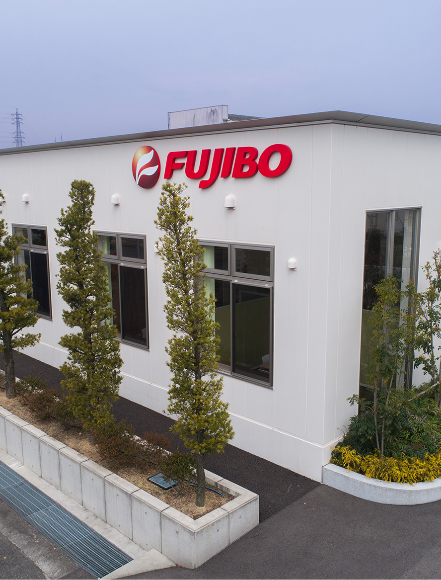
Production system with 4 plants in Japan and 1 plant outside Japan for BCP

The Oita Plant was completed in 2020 in addition to Tainan Plant to meet growing customer demands. We make full use of our exceptional production capacity with 5 plants to lead the industry in observing BCP.
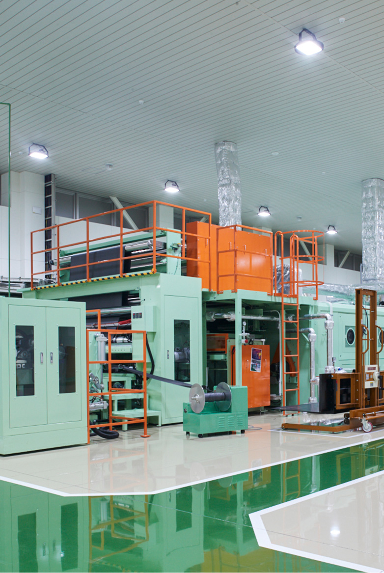
Well-established production facilities to enable development and manufacturing of a wide variety of polishing pads

We can quickly provide fully-customized polishing pads by our integrated production system covering from development to manufacturing of polishing pads.
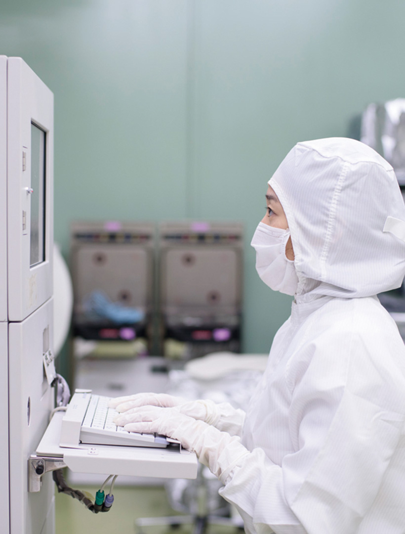
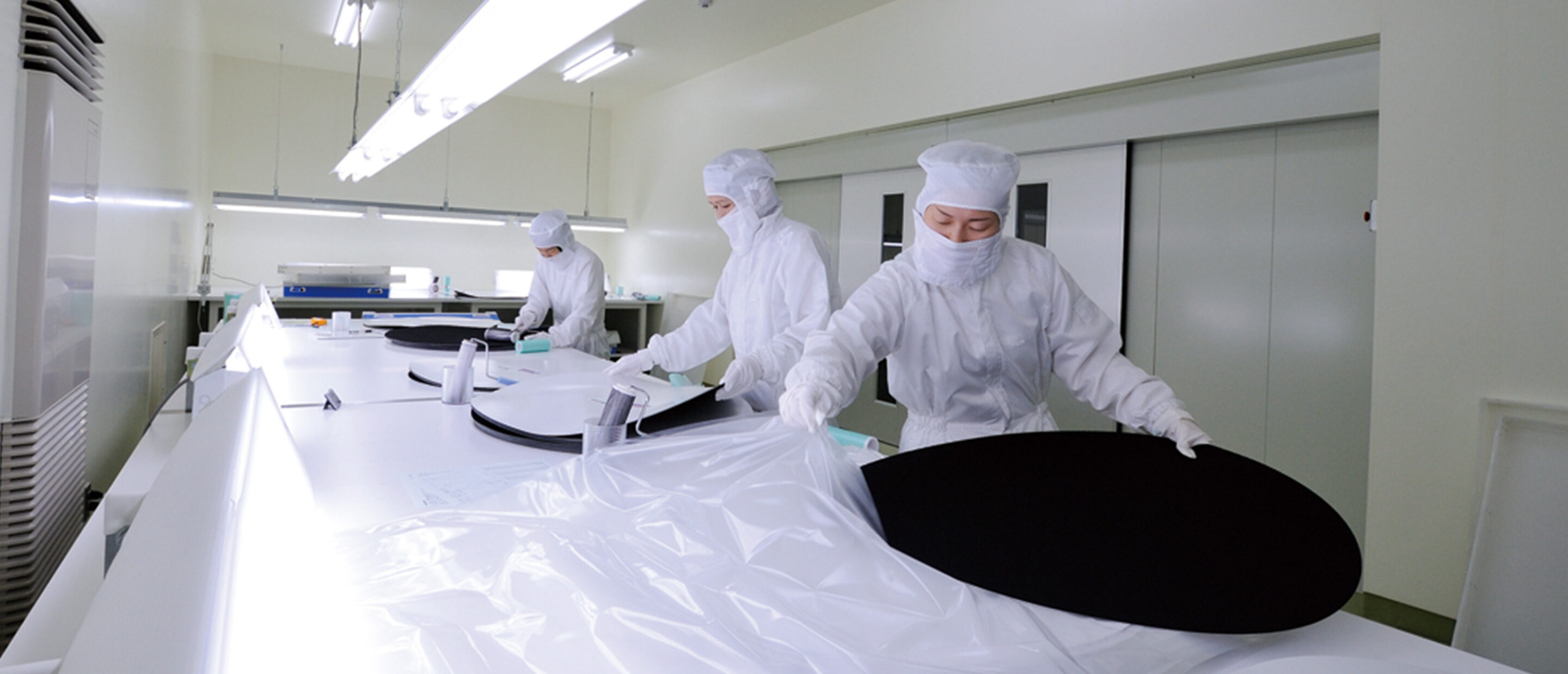
Clean environments which supports high quality

The Group uses various measuring equipment in clean rooms and has materialized high-level quality control that meets ISO9001 standards. At the same time, we have obtained ISO14001 certification and improved our environment management system.
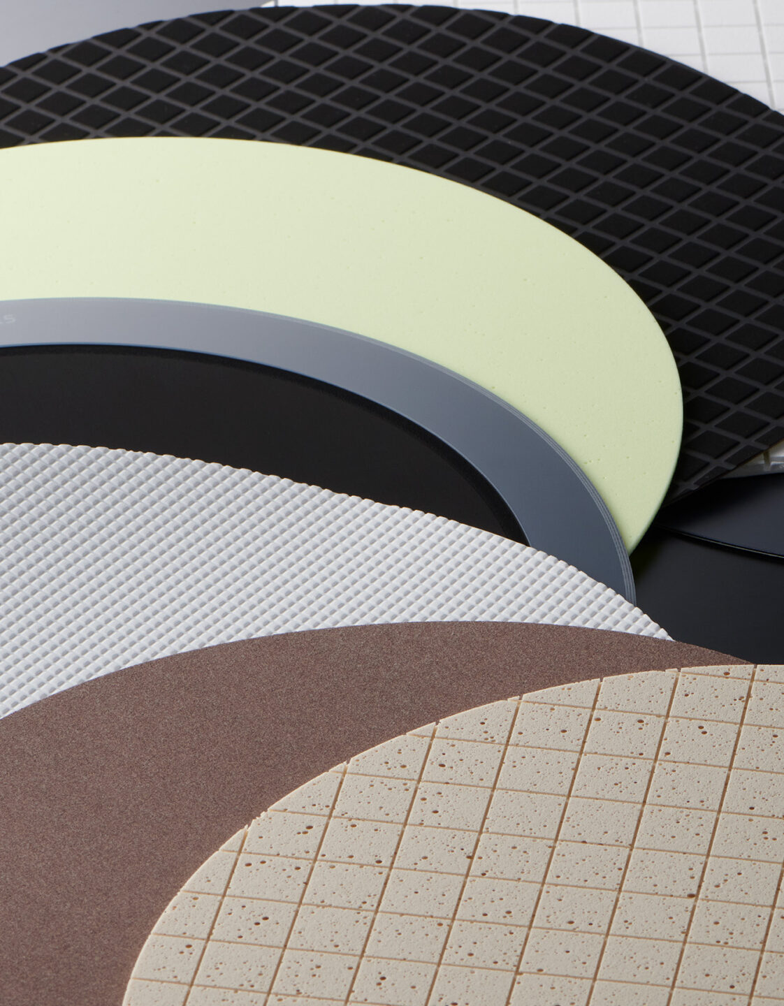

Polishing Pad
Product Information


A variety of products that enable ultra-high precision polishing
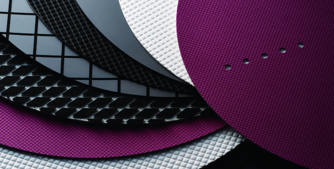
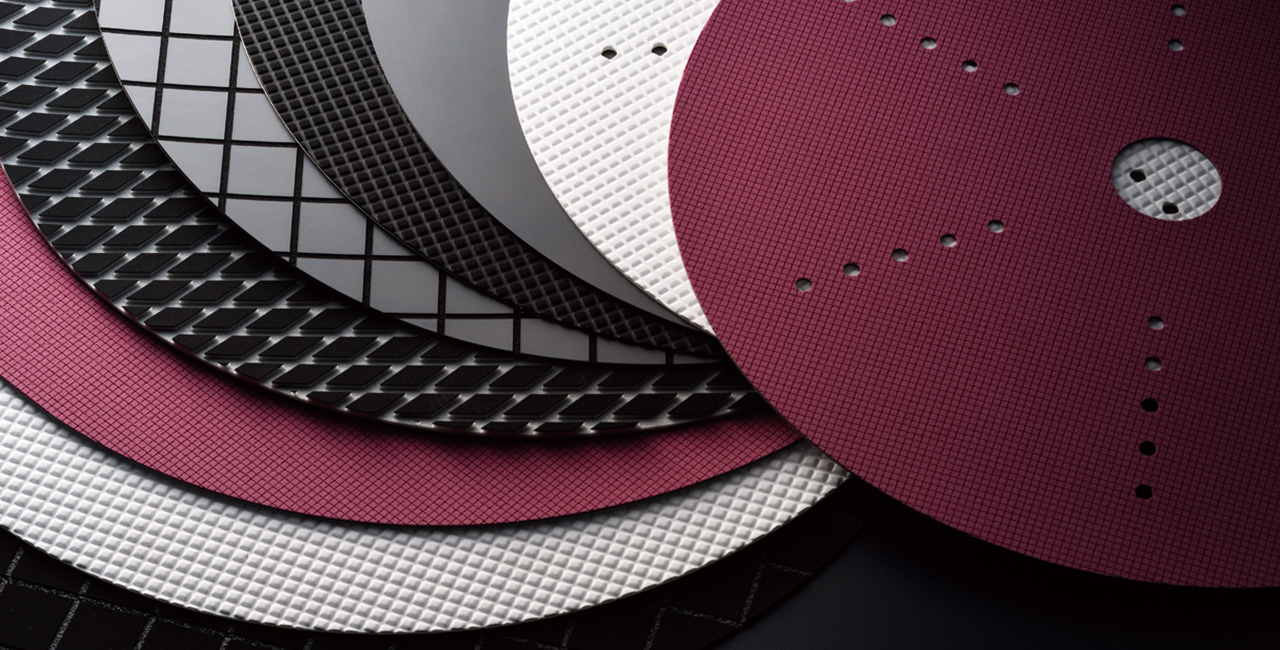
We offer a wide variety of POLYPAS® polishing pads for not only CMP, silicon wafers, hard disks and LCD glass but also for many other purposes.
We also ensure scratch-free, haze-free and high flatness necessary for its sophisticated polishing.
Gallery
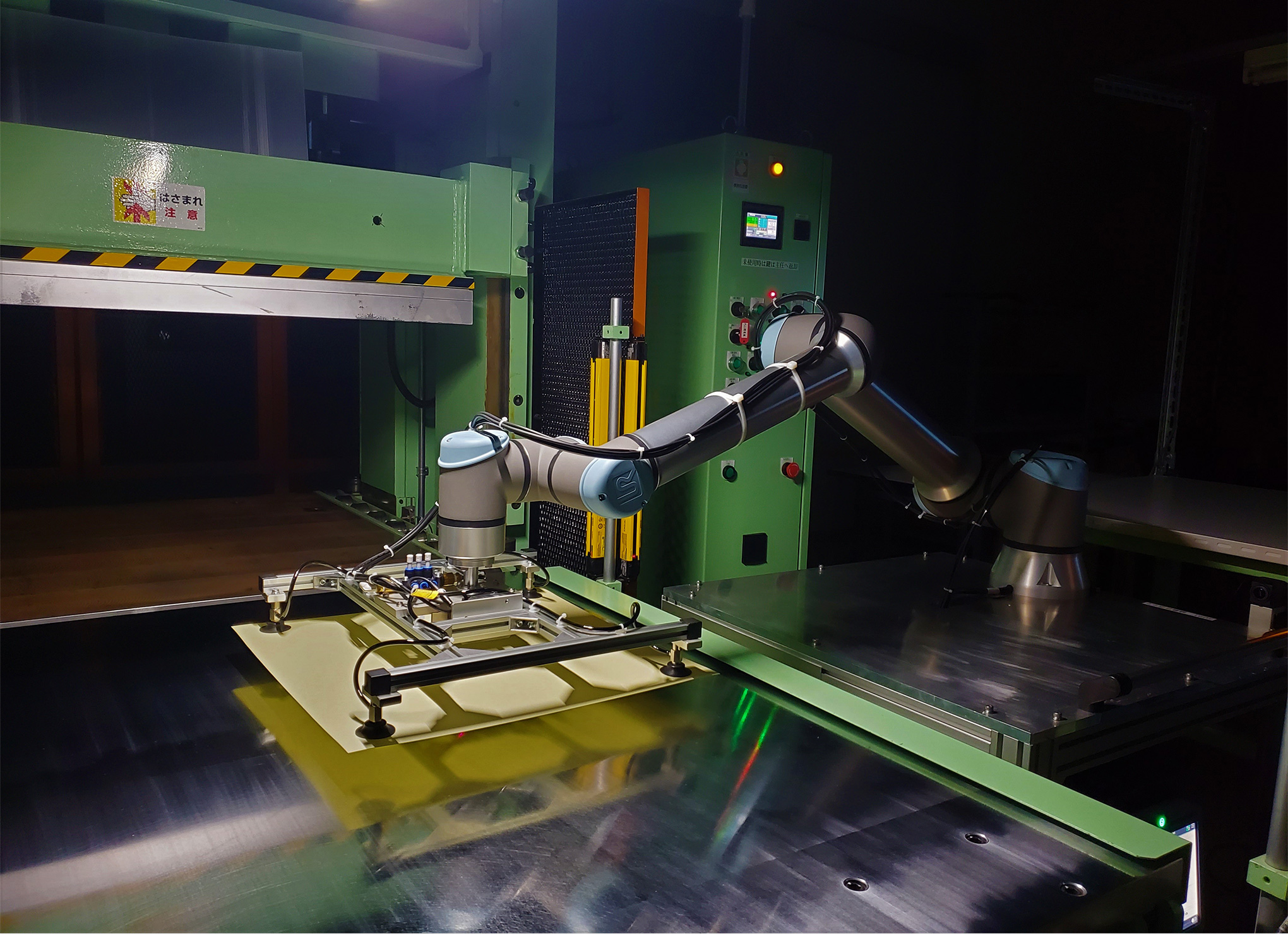
"Manufacturing processes promoting automatization and DX"
We seek to promote automatization in each process to enhance production efficiency.
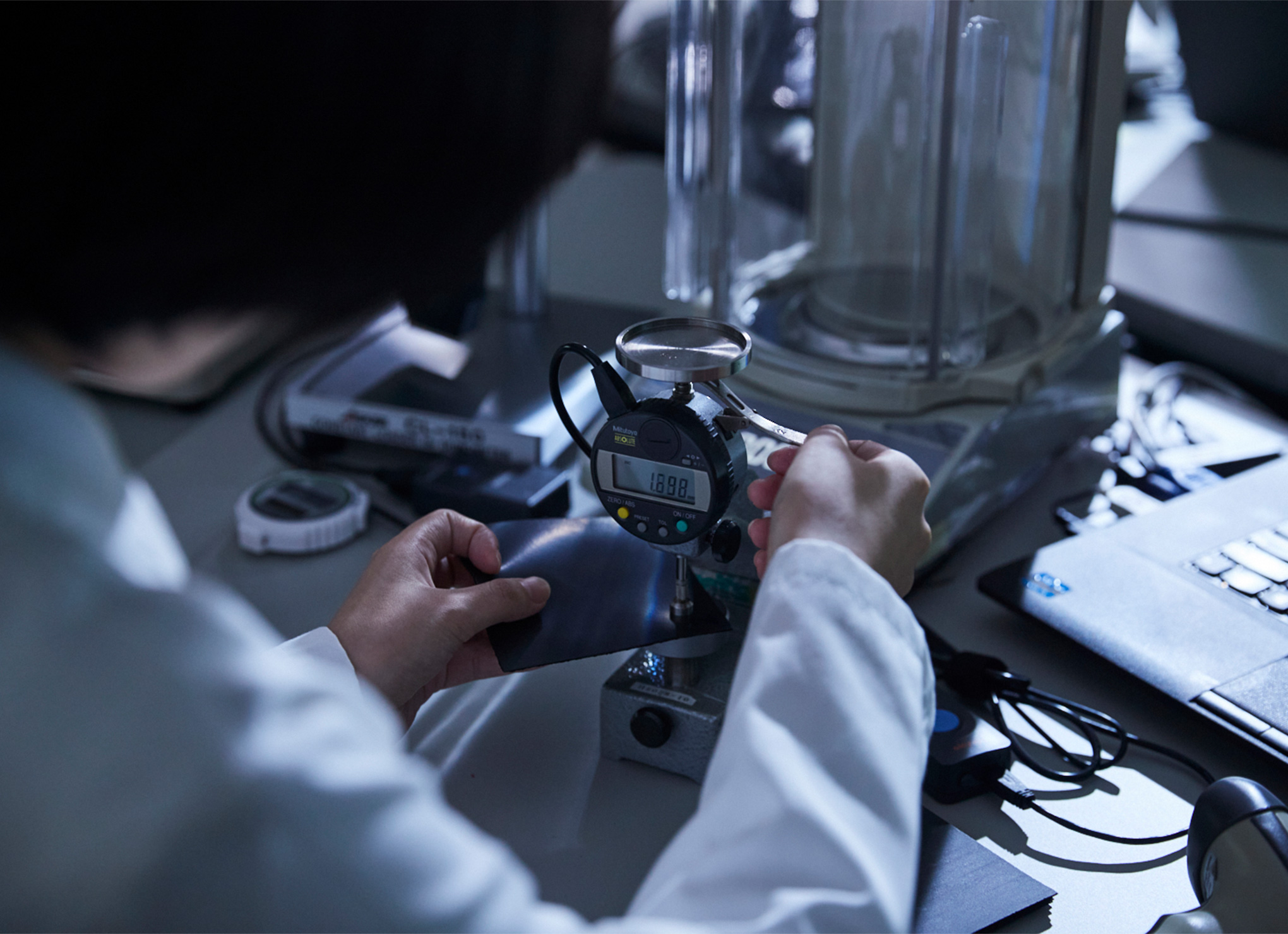
"High-level quality control"
In order to provide high quality polishing pads, we undertake extensive quality inspections and ensure that our polishing pads are of the unparalleled quality.
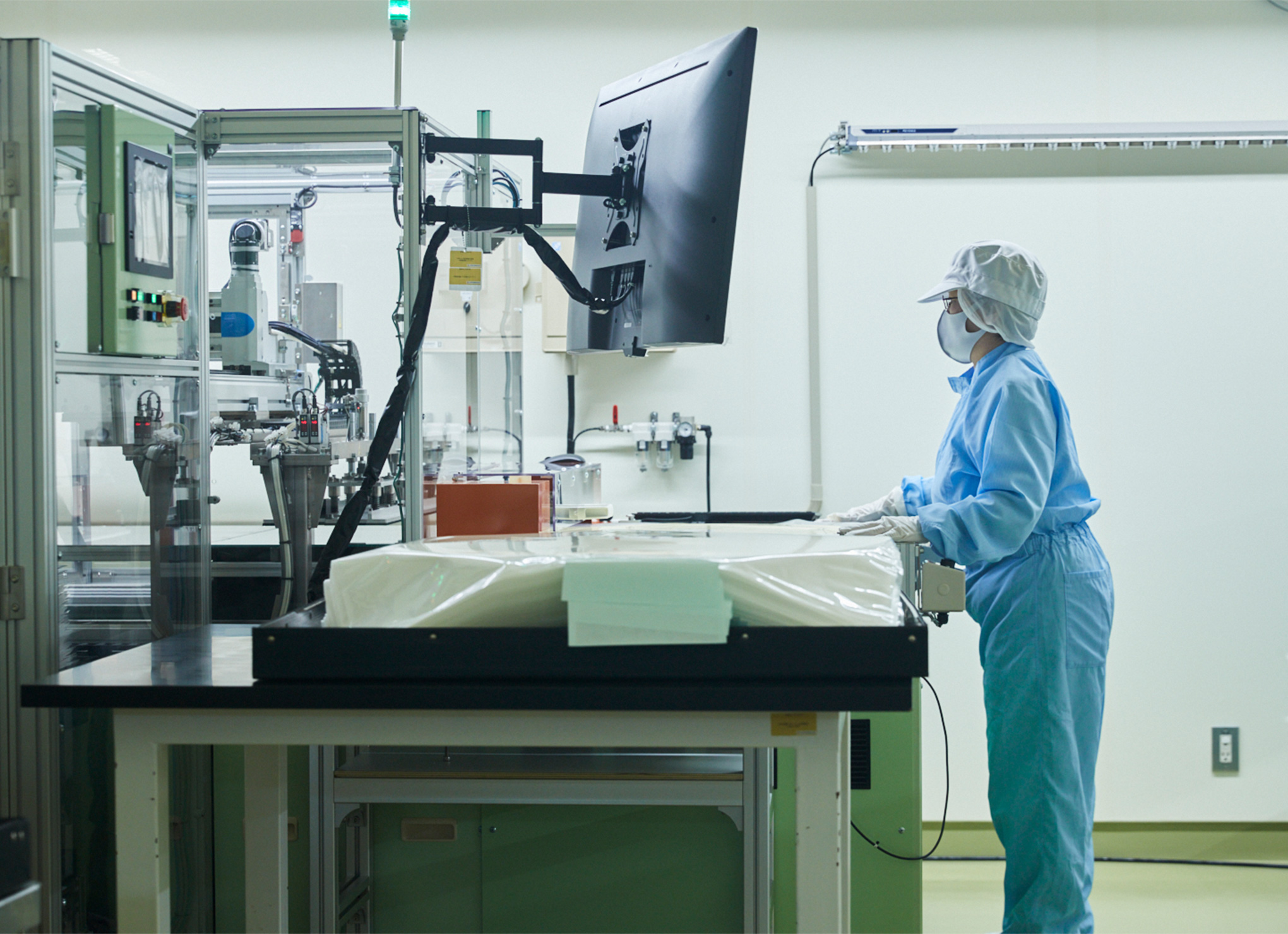
"Well-developed inspection system"
We have built up an AI inspection system to provide polishing pads that satisfy users.
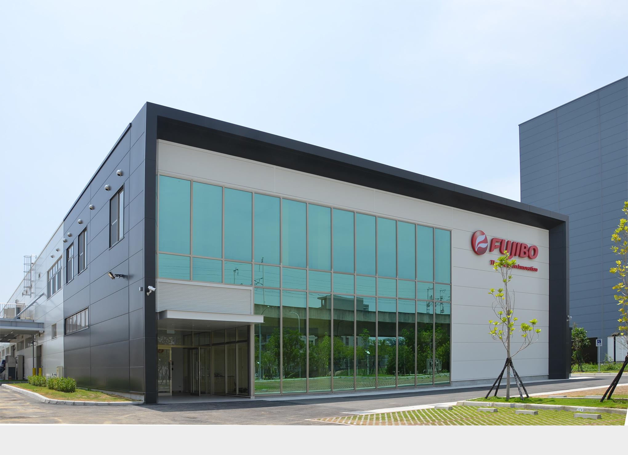
"Extending overseas production base"
To aggressively expand sales of polishing pads in the Taiwan market, we have established a base in Tainan.
Focus
On
-
Entering new fields and shift to aggressive patentingWe reinforce our marketing and accurately determine new markets, future growth potential and direction in the long-term, and expand our business as a comprehensive polishing pad manufacturer beyond just precision polishing pads and create new business by taking advantage of a "shift from defensive to aggressive patent strategy."
-
Acceleration and improvementWe accumulate knowledge and experience in manufacturing of polishing pads to improve analysis and polishing evaluation technologies, and whereby
we can become faster and better and will propose new polishing pads and polishing process at the best timing for customers and market needs.
-
Stable production systemWith five locations in and outside of Japan, we've created a reliable production system. We put more people in the rapidly growing polishing pad business and invest in development of the personnel.
Business
Firm


Environmental activities


To protect beautiful environment in Setouchi
We reinforce our wastewater treatment facilities and strictly manage them to deal with increased production of polishing pads. We established self-set standards in addition to the standards under the applicable laws including the Water Pollution Prevention Law and Act on Special Measures concerning Conservation of the Environment of the Seto Inland Sea and make capital investment for protecting the beautiful environment in Setouchi.
Product
Information
POLYPAS® polishing pad is designed for ultra-high precision polishing of silicon wafers and other materials including all semiconductor materials, metals and glasses.
